top of page

Device Circuit Co-Design Issues for Fast and Ultra Low Power CMOS and Beyond CMOS Technology
Harnessing Negative Capacitance Effect for Energy-Efficient Computing


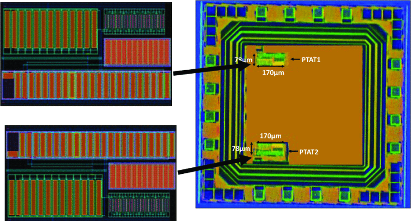
Fabrication of Rad-hard Low Power CMOS Temperature Sensor for Space Applications
GAATM TFET (a) Schematic (b) Cross-section.

TCAD simulation frame of single fin n-FinFET
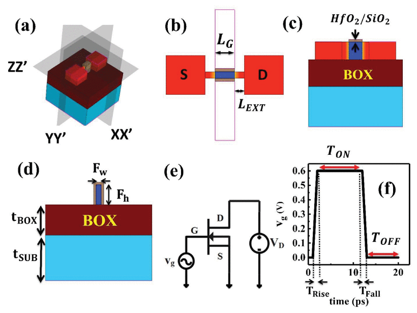
Device structure of (a) Single-Fin Tri-gate Fin-FET, (b) 3-Fin Tri-gate Fin-FET

Phase Noise Analysis of Separately Driven Ring Oscillators

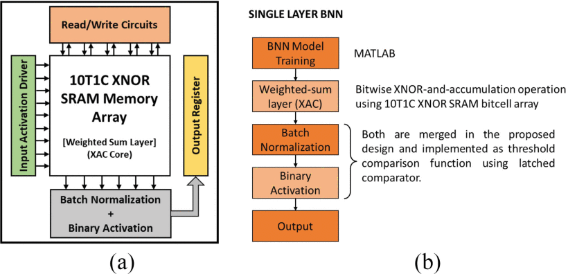
(a) A functional block diagram to implement BNN using the proposed XAC scheme. (b) Operation flowchart of single layer BNN.
(a) A functional block Proposed XAC scheme for in-memory computation in BNN. (a) Schematic of 10T1C XNOR SRAM bit-cell with its different operating modes, SRAM (M1) and XAC (M2) at different input/output cases. (b) Layout of the bit-cell. The MOM capacitor is laid on top of the SRAM cell hence no additional area is required. (c) Flowchart of CIM binary XNOR operation in 10T1C SRAM bit-cell.

bottom of page